Documentation
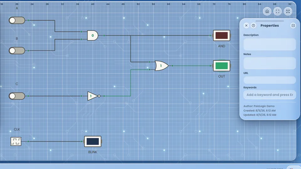
Getting started
- Creating a circuitA project holds one or more circuits, each shown as a tab along the circuit bar. You add a circuit with the + button on that bar, or through the menu Circuit → New. Give it a name — non-empty and unique within the project — and a fresh tab opens onto an empty canvas ready for parts. Switch between circuits by clicking their tabs.
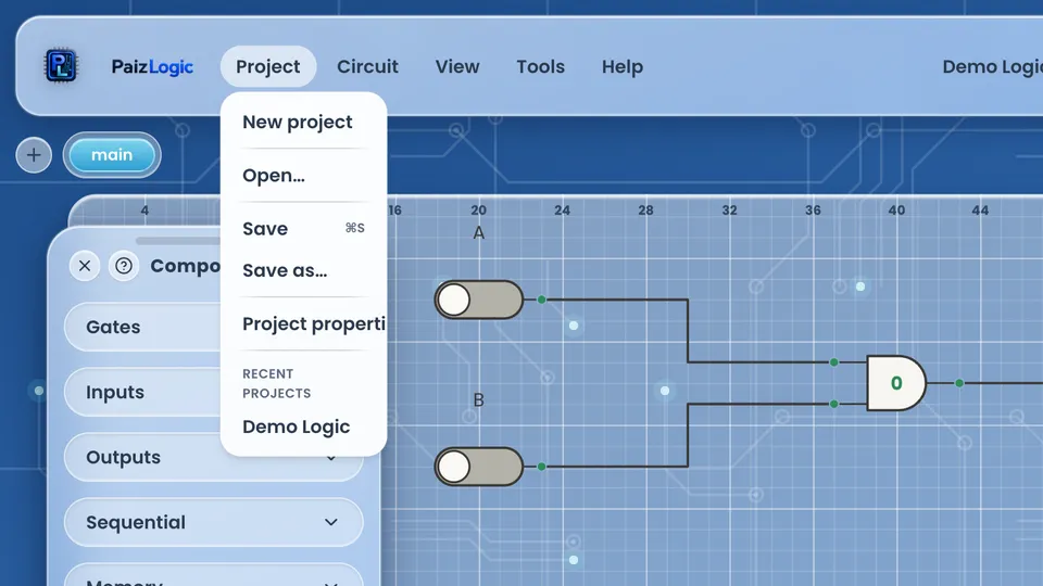
- Creating or opening a projectA project is the file that holds every circuit you work on, saved to your account. Project → New starts a brand-new, empty project — if the one you're on has unsaved changes it asks you to confirm first, so nothing is lost by accident. Project → Open shows a browser of your saved projects, organized into folders, each with a live preview thumbnail; click one to load it. Both actions live in the Project menu at the top-left of the top bar.
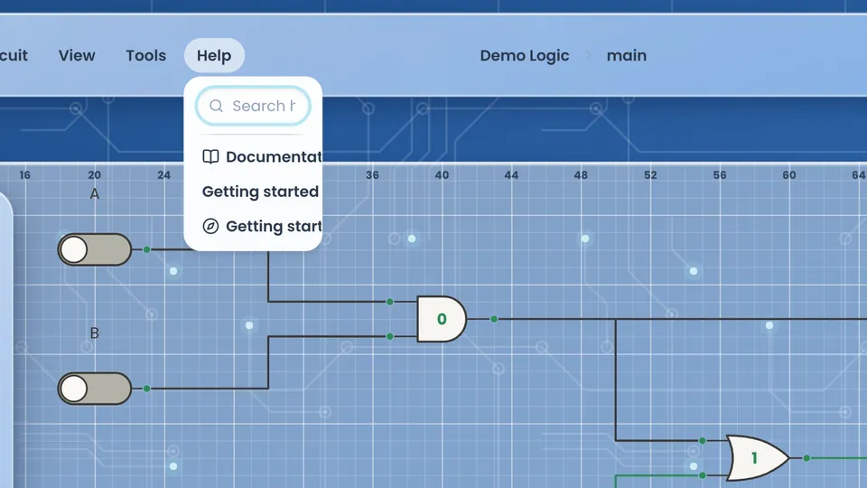
- Getting help for a componentEvery component in the palette has its own help topic — a description, worked examples and, for many, a truth table. The fastest way in is contextual: right-click any component in the Components panel and choose Show help for [name]; the Help panel opens straight to that topic, no searching required. You can reach the same content by typing the component's name into the Help menu's search box, or by browsing the Components chapter of the documentation index (Help → View documentation).
- Saving and autosaveNothing is written to your account until you save. Circuit → Save circuit (or ⌘S / Ctrl+S) writes just the circuit you're editing; Project → Save writes the whole project, and Project → Save As saves a copy under a new name or folder, leaving the original untouched. An asterisk next to the project name in the breadcrumb means there are unsaved changes. Autosave, off by default, is a separate setting in Preferences: turn it on and it silently re-saves the project on a timer between 1 and 30 minutes — but only once you've saved it by name at least once, and only when there's something new to write.
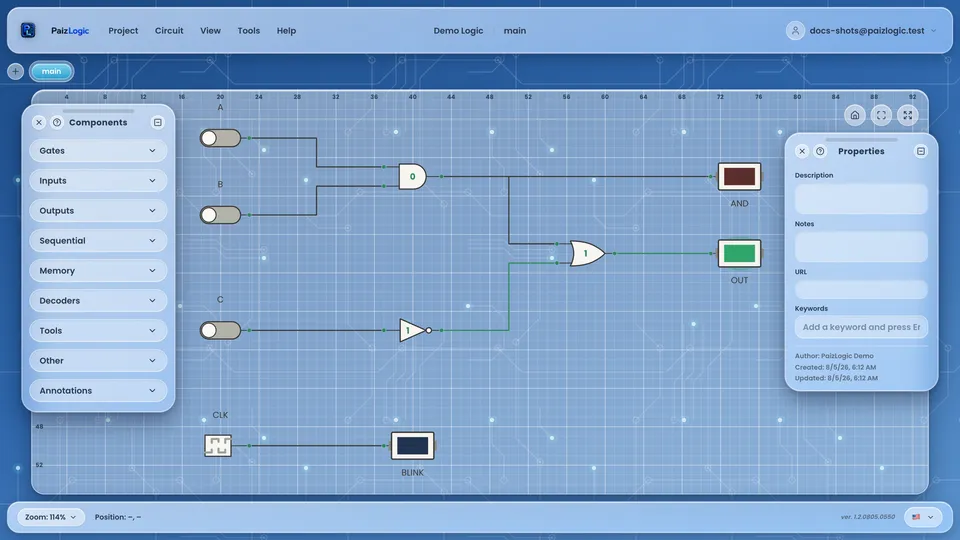
- Tour of the interfaceThe workspace is built from a fixed top bar and a set of floating panels around an infinite canvas. The top bar holds the Project, Circuit, View, Tools and Help menus on the left, the project/circuit breadcrumb in the middle, and your account menu on the right. The canvas is where circuits are built: drag components onto it, wire them together, and pan or zoom freely. Around it float the Components panel (the parts palette), the Properties panel (settings for whatever is selected), and, when opened, the Package, Toolbar, Align and Logic Analyzer panels — each can be shown or hidden from the View menu, dragged to a new position, and resized.
Interface
- Align panelThe Align panel aligns, distributes, and evenly spaces the selected elements on the canvas — left, center, right, top, middle, or bottom alignment, plus horizontal and vertical distribution and spacing with a configurable gap. It appears automatically when you select 2 or more elements, and can also be pinned open from the View menu.
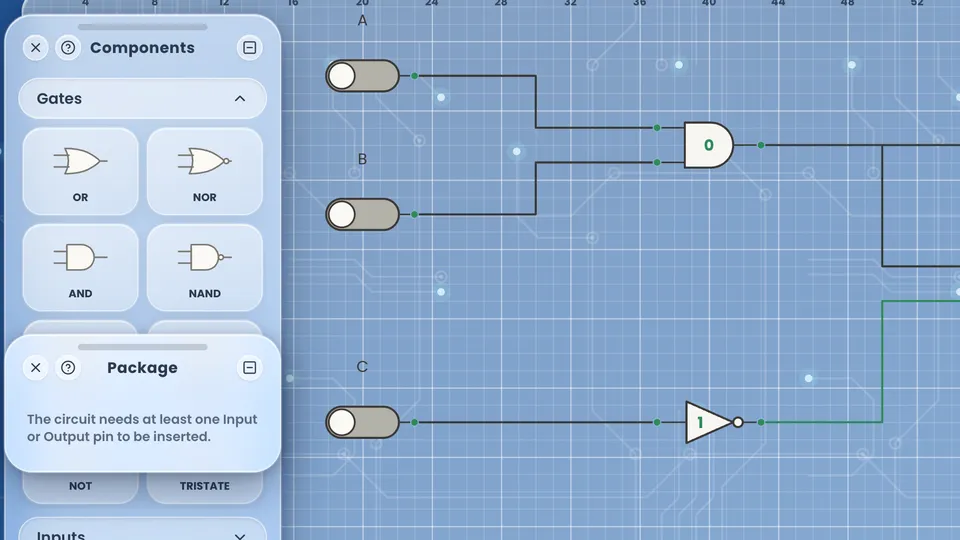
- Components panelThe Components panel is the palette of every element you can place on the canvas, organized by category: gates, inputs, outputs, sequential elements, decoders, other components, and annotations. Drag a component onto the canvas to place it, or double-click it to insert it automatically centered in the area you're currently viewing. Right-click a component for a quick menu, including a link to its own help topic. The full catalog, grouped by category, is listed below.
- Logic Analyzer panelThe Logic Analyzer panel shows a live timing diagram of up to 16 signals, one per Logic Analyzer probe placed on the canvas. Each channel can be enabled or disabled, relabeled, and recolored; the diagram scrolls in real time as the simulation runs, making it easy to compare timing relationships between signals.
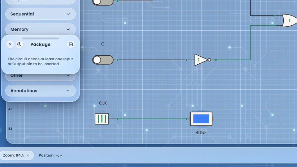
- Package panelThe Package panel defines how the active circuit looks when encapsulated as a reusable component: the body shape (linear, square, or hexagonal), which luminous elements surface as lights on the body, free-form silkscreen labels, and the position of each terminal. Terminal placement is automatic by default; a manual mode lets you drag terminals to reorder or relocate them, within the limits of the active shape.
- Preferences windowPreferences opens from the account menu and controls three things: the interface language, which panels are shown by default when a project opens, and autosave. Switching Language here changes the UI immediately, the same as picking it from elsewhere in the app. The Default panels checklist sets which of Components, Properties, Package and Toolbar are visible on a fresh project — it does not affect panels you have already opened in the current session. Every change is written the moment you press Save.
- Profile windowProfile opens from the account menu in the top-right corner (click your name or avatar) and edits the personal information tied to your account: first and last name, country, gender, a short bio, and an avatar photo. Email is shown but read-only, since it comes from your sign-in provider. Changes are written when you press Save; closing the dialog without saving discards them.
- Properties panelThe Properties panel edits the currently selected element: bit width, number of inputs, propagation delay, color, label, and other component-specific fields. When nothing is selected, it shows the active circuit's own metadata instead — description, notes, reference URL, and search keywords — so you can document the circuit itself.
Wiring
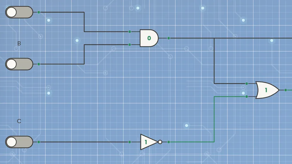
- How to wire two componentsA wire carries a signal from one component's output port to another's input port. You draw one by dragging from an output to an input; when the pointer reaches a compatible port the wire snaps into place. Once connected, the wire is colored by the value it carries: green means logic HIGH (1), a dark line means logic LOW (0), and red marks a floating wire that is driven by nothing.
- Using buses (multi-bit wires)A bus is a single wire that carries several bits at once, so one connection moves a whole binary number instead of one bit. You create a bus by setting a component's bit width above 1; buses render as a dotted line to tell them apart from plain 1-bit wires. To reach an individual bit, break the bus apart with a Splitter; to combine bits back into a bus, gather them the opposite way. A bus and a 1-bit wire cannot be joined directly — their widths must match.
Subcircuits
- Creating a sub-circuitA sub-circuit packages a circuit into a reusable block, like a custom chip. You build a normal circuit whose Input and Output pins become the block's terminals, then turn it into a sub-circuit of a parent with Circuit → New sub-circuit, or by right-clicking a tab and choosing Insert. The sub-circuit becomes an exclusive child of that parent, listed in the parent tab's ↓ dropdown. Select it there to drill in and edit it; a breadcrumb shows Project → Circuit → Sub-circuit so you always know where you are.
- Subcircuit insertion rulesThree official rules govern what may be inserted into what. (a) A circuit may insert ANY other circuit, as long as doing so does not create a recursive cycle. (b) A circuit may also insert its OWN subcircuits, reusing them within the same parent. (c) A sub-circuit may NOT insert any circuit or subcircuit — nesting is one level deep from each editing context, so while you edit a subcircuit the Insert command is disabled. Together these rules keep the hierarchy finite and guarantee the flattener always terminates.
- Terminals and package exposureA subcircuit's OUTPUT terminals are usable by the parent's wiring — you can connect them to gates, components, or even another subcircuit within the same parent. But they are NOT exposed on the parent's package (its footprint UI) unless they are wired to one of the parent's OWN Output terminals. Package pins derive only from a circuit's own Input and Output components, never directly from a subcircuit's terminals. So a subcircuit output that stays internal drives the parent's logic silently, while one routed to a parent Output becomes a visible pin on the parent's package.
- What a subcircuit isA subcircuit is a circuit instantiated inside another circuit, the way a component is placed on the canvas. It is stored exclusively under its parent and never appears in the main circuit list; you reach it through the down (↓) dropdown on the parent's tab. Opening a subcircuit drills into it as the active, editable circuit, with a breadcrumb Project › Parent › Subcircuit so you always know where you are and can click any ancestor to return.
Menus
- Circuit menuThe Circuit menu works with the circuits inside the project. Create a new top-level circuit, add a new sub-circuit inside the active circuit, import a circuit, or save the active circuit.
- Help menuThe Help menu is the way into the documentation. It offers a search box, opens the floating Help panel, and opens the full documentation index.
- Insert (Circuit menu)The Insert row in the Circuit menu opens a flyout listing every other circuit and sub-circuit in the project that can be placed as a live instance on the active canvas — the same flyout is also available from the canvas' right-click menu when nothing is selected. Picking one drops a package instance centered in the current view, wired to the same live circuit it represents.
- Project menuThe Project menu manages the whole project file. From here you create a new project, open an existing one, save or save the current one under a new name, reopen a recent project, and edit the project's properties.
- Tools menuThe Tools menu is reserved for analysis and utility tools. It is a placeholder for now and will host heavier circuit-analysis features in a future release.
- View menuThe View menu shows or hides the workspace panels and controls the Align panel. A check mark next to a panel means it is currently visible.
Components
- 16-Segment DisplayAn alphanumeric display whose sixteen LED segments, including diagonals and split horizontal bars, can form every digit 0-9 and every uppercase letter A-Z, unlike the digits-only 7-segment. In PaizLogic it reads a 7-bit bus and shows the matching ASCII character. Real parts such as the Maxim MAX6954 store a full 16-segment ASCII font on-chip and drive the display from a serial word, the same idea PaizLogic hides behind a single 7-bit input.
- 7-Segment DisplayA numeric display built from seven bar-shaped LEDs, labeled a through g, arranged in a figure-eight. In PaizLogic it takes a 4-bit bus on its single input and lights the segment pattern for that value's hexadecimal digit, 0 through F. Internally, choosing which segments to light for each digit is a combinational function of the four input bits, exactly the job that a BCD-to-seven-segment decoder chip does in real hardware.
- AND gateThe AND gate outputs 1 only when every input is 1; if any input is 0 the output is 0. It implements logical conjunction (A · B) and is the building block for enabling, masking, and coincidence detection.
- BCD to 7-segment decoderTurns a 4-bit BCD digit into the seven segment lines that draw it. The input is a number from 0 to 9; the outputs a through g each drive one bar of the display. It exists so you do not have to work out, gate by gate, which bars light up for which digit — that mapping is the whole component.
- Bit selectorA bit selector extracts a single bit from an input bus. The value on the selector lines is an index into the bus, and the output is the addressed bit. It is effectively a multiplexer whose data inputs are the individual wires of one bus, and it is the natural way to test or route one bit of a word.
- Bus MergerA bus is a bundle of wires that carry a multi-bit value as one line. The Merger composes N individual 1-bit lines into one outgoing N-bit bus, so input i becomes bit i of the bus. It performs no logic and adds no delay: it is purely a wiring convenience that lets you combine separately-driven signals into a single bus line. It is the Splitter's exact counterpart — where the Splitter breaks a bus apart, the Merger puts one back together.
- Bus SplitterA bus is a bundle of wires that carry a multi-bit value as one line. The Splitter decomposes an incoming N-bit bus into N individual 1-bit lines, so bit i of the bus becomes output i. It performs no logic and adds no delay: it is purely a wiring convenience that lets you route or observe each bit separately. Because the simulator already supports fanout, the same signal source can feed the bus and every split bit stays in sync with it.
- ClockThe clock is a free-running signal source that toggles its output automatically between 0 and 1 at a fixed period, producing a 50% duty-cycle square wave. It needs no inputs; you only set the period. The clock is the heartbeat of every synchronous circuit: its rising edges define the instants at which flip-flops, counters and shift registers update, so every sequential element you place will usually trace back to a clock.
- CounterThe counter is a ready-made synchronous up-counter. On each rising clock edge it increments its stored value and presents it on the Value bus; when the count reaches the Max Value input it wraps back to 0 on the next edge. An asynchronous Reset forces the count to 0 immediately, overriding the clock, and a Zero output flag goes high whenever the count is 0. It packages a whole chain of flip-flops and gates into one block, ideal for timing, addressing, event tallies and sequencing.
- D Flip-FlopThe D (data) flip-flop is the workhorse memory element of synchronous digital design. On every rising edge of the clock it samples the D input and stores it in the output Q, holding that value until the next edge. Asynchronous PRE (preset) and CLR (clear) inputs force Q to 1 or 0 immediately regardless of the clock, with CLR winning if both are asserted. Because it captures data only at a well-defined instant, the D flip-flop is the standard building block for registers, pipelines and finite state machines.
- D LatchThe D latch is a level-sensitive storage element, the transparent cousin of the D flip-flop. While the Enable input is high the latch is 'transparent' and Q simply follows D; when Enable goes low the latch 'closes' and holds the last value D had. Asynchronous PRE and CLR force Q immediately (CLR wins). Because it responds to the whole high level of Enable rather than to a single edge, a latch is faster and smaller than an edge-triggered flip-flop but far more sensitive to input glitches, so it is used deliberately, for example in two-phase clocking and register files.
- Demultiplexer (DEMUX)A demultiplexer is the inverse of a multiplexer: it forwards a single data input to exactly one of several outputs, chosen by the select lines. All non-selected outputs stay inactive. A DEMUX with n select lines drives one of 2^n outputs and is the basic data-distribution element.
- DIP switchA bank of independent toggle switches in a single package. Each position has its own output pin and its own state, and you flip one by clicking it. It is the tidy way to feed a circuit several fixed inputs at once — the kind of settings you set before running and rarely touch again.
- EEPROMNon-volatile memory: it behaves exactly like the RAM (combinational read, synchronous write on a rising CLK edge with WE HIGH, asynchronous RST clear) but its contents persist — simulated writes are stored with the circuit, and the cells can also be authored by hand in the Properties panel, just like the ROM.
- Ground (GND)A constant source whose output is always logic LOW (0). It represents the reference rail, ground or GND, the zero-volt node that a logic family reads as a false or deasserted level. Use it wherever a signal must be permanently 0: to tie an unused input low, to hold an active-low clear asserted, or to supply a constant 0 operand to logic.
- Image AnnotationThe Image annotation places a picture on the canvas purely for documentation. It has no input or output terminals and takes no part in simulation, so it never affects logic values or timing. Use it to embed a datasheet excerpt, a pin-out, a reference photo or a project logo next to the circuitry it explains. Like all annotations, it is a visual aid whose only job is to make the diagram easier to read and understand.
- Input SourceA user-driven signal source. Each bit is an independent switch you toggle by hand: a bit set to 1 drives its wire to logic HIGH, a bit set to 0 drives it to logic LOW. With a bit width above 1 the terminals form a bus that carries a binary number, and the whole source can be mapped to a package pin so the finished circuit exposes it as an external input.
- JK Flip-FlopThe JK flip-flop is the most versatile of the clocked flip-flops. On each rising clock edge its two inputs select one of four actions: J=0 K=0 holds, J=1 K=0 sets Q to 1, J=0 K=1 resets Q to 0, and J=1 K=1 toggles Q. It removes the forbidden state of the SR flip-flop by redefining that combination as a useful toggle. Asynchronous PRE and CLR override the clock (CLR wins). Any other flip-flop can be built from a JK, which is why it is a favourite teaching and counter-design primitive.
- Junction nodeA branch point on a wire. The node takes the signal arriving on its input and repeats it, unchanged, on up to three branches, so one source can reach several destinations. It carries no logic and adds no delay — it is the drawing of a shared connection, not a component that does anything to the signal.
- LED (Light-Emitting Diode)A single-bit luminous output. The LED lights up in its selected color when its input carries a digital 1 (HIGH) and stays dark on a 0 (LOW). It is the simplest way to visualize a logic signal on the canvas: wire any output to it and watch the level. In real hardware an LED is a semiconductor diode that emits light when current flows through it in the forward direction, so it only cares about the level on its single input, not about buses.
- Line decoderA decoder drives exactly one of its output lines high, selected by the binary value on its input. An n-bit input activates one of 2^n outputs, producing a one-hot pattern. Decoders translate compact binary codes into individual control lines and are the counterpart of encoders.
- Logic Analyzer ProbeA single-input tap that samples one node on the canvas and streams its value to a channel of the Logic Analyzer (Tools menu). It performs no logic and drives nothing back onto the circuit — wiring a Probe's input to a node never changes that node's behavior, it only observes it. Place up to 16 probes, one per channel; each one renders in the analyzer's timing diagram in the probe's own color, so you can tell which trace belongs to which node at a glance.
- LSB detectorThe LSB detector reports the index of the least-significant bit set to 1 in the input bus, with an enable flag that is high only when at least one bit is set. Scanning from the bottom, it isolates the lowest one, the operation behind find-first-set and allocator logic.
- Magnitude comparatorCompares two unsigned buses A and B and reports the result on three separate outputs: A>B, A=B and A<B. Exactly one of them is HIGH at any moment, because two numbers are always either greater, equal or lesser. It answers the question a subtractor only implies, and it answers it without producing a difference you would then have to interpret.
- MSB detectorThe MSB detector reports the index of the most-significant bit that is set to 1 in the input bus, together with an enable flag that is high only when at least one bit is set. Scanning from the top, it locates the leading one, which is the classic priority function used for normalization and magnitude estimation.
- Multiplexer (MUX)A multiplexer routes one of several data inputs to a single output. The binary value on the select lines addresses which input is connected, so a MUX with n select lines chooses among 2^n data inputs. It is the fundamental data-steering and data-selection building block of digital systems.
- NAND gateThe NAND gate is an AND followed by an inverter: the output is 0 only when every input is 1, and 1 otherwise. NAND is functionally complete — any Boolean function can be built from NAND gates alone — so it is one of the most important gates in real hardware.
- NOR gateThe NOR gate is an OR followed by an inverter: the output is 1 only when every input is 0, and 0 if any input is 1. Like NAND, NOR is functionally complete — any logic circuit can be built from NOR gates alone.
- NOT gate (inverter)The NOT gate, or inverter, has a single input and outputs its logical complement: 1 becomes 0 and 0 becomes 1 (Y = Ā). It is the simplest gate and appears everywhere signals must be negated, restored, or delayed.
- OR gateThe OR gate outputs 1 when at least one input is 1, and 0 only when every input is 0. It implements logical disjunction (A + B) and is used for combining conditions, alarms, and any 'at least one' decision.
- Output TerminalA read-only probe that displays the value present on the wire or bus feeding it. It never drives a signal of its own; it only reports whether its input is logic HIGH (1) or logic LOW (0), or the binary number carried by a multi-bit bus. Like an input, an output can be mapped to a package pin so the finished circuit exposes it as a named external result.
- Parity checkerA parity checker recomputes the parity of a received word and compares it against the transmitted parity bit. A mismatch means an odd number of bits flipped, so it raises an error flag. Single-bit parity detects any odd-weight error but cannot locate or correct it.
- Parity generatorA parity generator computes a single check bit from an input bus by XORing all of its bits. For even parity the bit makes the total number of ones even; for odd parity it makes the total odd. Appended to the data, this bit lets a receiver detect any single-bit corruption.
- PISO Shift RegisterA PISO (parallel-in, serial-out) shift register does the opposite of a SIPO. Asserting Reset loads all N parallel D inputs into the register at once; then, on each rising clock edge, it shifts the word right and presents one bit at a time on the single serial Q output, least-significant bit first. After N clocks the whole word has been streamed out. PISO registers turn a parallel word into a serial stream, the transmitting half of parallel-to-serial conversion and the foundation of serial data links.
- Power (VCC)A constant source whose output is always logic HIGH (1). It represents the supply rail, VCC, the positive voltage that a logic family reads as a true or asserted level. Use it wherever a signal must be permanently 1: to tie an unused input high, to hard-wire an enable on, or to supply a constant operand to logic.
- Priority encoderA priority encoder outputs the binary index of the highest-priority input that is active, ignoring any lower-priority inputs that are also active. A valid flag distinguishes the all-zero case from a genuine index of 0. It is the inverse of a decoder and the standard way to arbitrate competing requests.
- Push ButtonA momentary source: it outputs logic HIGH (1) only while you hold it pressed and springs back to logic LOW (0) the instant you release. This mirrors a real push button wired with a pull-down resistor, whose default idle state is 0 and which is pulled to 1 only while the contact is closed. It is the tool of choice for generating a short, deliberate pulse, such as a manual clock tick or a one-shot trigger.
- RAMRandom-access memory: reads are combinational (the output always shows the word at ADDR) and writes are synchronous — on a rising CLK edge with WE HIGH, the DIN word is stored at ADDR. RST asynchronously clears every cell. The memory always powers up zeroed; its contents are runtime state and are not saved with the circuit.
- Region AnnotationThe Region annotation is a dashed rectangle used to group and highlight an area of the circuit. Like the other annotations it carries no signal and takes no part in simulation. You size it with its width and height and tint it with the 24-color design palette. By drawing a visible boundary around a set of components, a region exploits the way our perception groups things enclosed by a common border, making functional blocks instantly recognizable.
- RGB LEDA three-input luminous output that mixes red, green and blue light additively to produce a color. Each of its three inputs controls one channel. With single-bit inputs each channel is simply on or off, giving the eight primary/secondary colors of additive mixing (red + green = yellow, red + blue = magenta, green + blue = cyan, all three = white). Real full-color RGB LEDs go further: they drive each channel with 8 bits of brightness, so 8 + 8 + 8 = 24 bits encode 256 x 256 x 256 = 16,777,216 colors, the origin of '24-bit true color'.
- RGB LED MatrixThe RGB LED Matrix is a rectangular array of pixels, each holding a 24-bit color (8 bits red + 8 bits green + 8 bits blue, following the sRGB channel model). It is a stateful display sink: it drives no outputs, but it remembers every pixel's color until you overwrite it. Three independent write methods let you address the matrix at different granularities, and they are applied low-to-high in each pass so a later method overwrites an earlier one on the same cell. Colors are masked to 24 bits before storage.
- ROMRead-only memory: a table of pre-authored words addressed by the ADDR bus. While EN is HIGH the output presents the word stored at the current address; while EN is LOW the output floats (high impedance), so several memories can share one data bus. The contents are edited in the Properties panel as hexadecimal words and cannot be changed by the circuit itself.
- SIPO Shift RegisterA SIPO (serial-in, parallel-out) shift register accepts one bit at a time on its serial DATA input and shifts the stored word left on every rising clock edge, so the newest bit enters position Q0 and older bits move up toward Q(N-1). After N clocks the whole word is available in parallel on the N Q outputs. An asynchronous Reset clears the register to 0. SIPO registers turn a single serial line into a parallel word, the receiving half of serial-to-parallel conversion.
- SR Flip-FlopThe SR (set-reset) flip-flop is the simplest clocked storage cell. On a rising clock edge S=1 sets Q to 1, R=1 resets Q to 0, and S=R=0 holds the previous value. The combination S=R=1 is forbidden because it asks the cell to be set and reset at once, leaving Q and Q' undefined. Asynchronous PRE and CLR act immediately (CLR wins). The SR flip-flop is the conceptual ancestor of all the others and maps directly onto the cross-coupled gate latch found inside real memory bits.
- T Flip-FlopThe T (toggle) flip-flop has a single data input T. On each rising clock edge it inverts its stored output Q when T is 1 and keeps it unchanged when T is 0. Asynchronous PRE and CLR set or clear Q immediately (CLR wins). Because a stream of toggles naturally halves a frequency, the T flip-flop is the classic element for binary counters and clock dividers, and it is functionally a JK flip-flop with J and K tied together.
- Text AnnotationThe Text annotation is a free-form label placed on the canvas for notes, titles and callouts. It has no terminals and no logic role, so it never affects simulation. You control its font size, font family (Poppins, monospace or serif), font style (normal, bold, italic, bold-italic) and color from the 24-color design palette. Clear labelling turns a wiring diagram into a document that explains itself, which is the whole point of an annotation.
- Toggle SwitchA latching source: one click flips it between logic LOW (0) and logic HIGH (1), and it holds that state until you click again. Where a button returns on its own, a switch remembers, which makes it the natural choice for a setting or mode that must stay put. It models a real single-pole toggle, whose defined level depends on whether it is wired with a pull-up or a pull-down resistor.
- Tri-state bufferA switchable connection rather than a logic function: while EN is HIGH the output Q repeats the input D unchanged, and while EN is LOW the output stops driving altogether and floats at high impedance (Z). That third state is what lets several devices share one bus — each drives it only when enabled, and the rest stay out of the way.
- XNOR gate (exclusive NOR)The XNOR gate is the inverse of XOR: it outputs 1 when its inputs are equal and 0 when they differ; with more inputs it outputs 1 for an even number of 1s. It computes A ⊙ B and is the natural equality-comparison and even-parity element.
- XOR gate (exclusive OR)The XOR gate outputs 1 when its inputs differ and 0 when they are equal; with more inputs it outputs 1 for an odd number of 1s. It computes A ⊕ B and is the heart of adders, parity checkers, and comparators.
Reference
- Align bottomMoves every selected component so their bottom edges line up on the same horizontal line - the bottom edge of the lowest component.
- Align horizontal centersLines up the selected components on a shared vertical axis so their horizontal centers match, without changing their vertical positions.
- Align leftMoves every selected component so their left edges line up on the same vertical line - the left edge of the leftmost component.
- Align rightMoves every selected component so their right edges line up on the same vertical line - the right edge of the rightmost component.
- Align topMoves every selected component so their top edges line up on the same horizontal line - the top edge of the highest component.
- Align vertical centersLines up the selected components on a shared horizontal axis so their vertical centers match, without changing their horizontal positions.
- Distribute horizontallyKeeps the leftmost and rightmost components fixed and repositions the ones in between so the horizontal gaps between them are equal.
- Distribute verticallyKeeps the topmost and bottommost components fixed and repositions the ones in between so the vertical gaps between them are equal.
- Set horizontal spacingArranges the selected components left to right with a fixed horizontal gap between them, taken from the gap value in the panel.
- Set vertical spacingStacks the selected components top to bottom with a fixed vertical gap between them, taken from the gap value in the panel.