NOT gate (inverter)
The NOT gate, or inverter, has a single input and outputs its logical complement: 1 becomes 0 and 0 becomes 1 (Y = Ā). It is the simplest gate and appears everywhere signals must be negated, restored, or delayed.
Single inverter
Wire one input A and read Y. The output is always the opposite of the input, as the two-row truth table shows. The small bubble on the symbol marks the inversion.
| A | Y |
|---|---|
| 0 | 1 |
| 1 | 0 |
Double inverter as a buffer
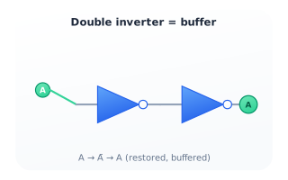
Two inverters in series cancel each other: A → Ā → A. The logic value is restored, but the signal is buffered — refreshed and slightly delayed. Designers use inverter pairs to strengthen weak signals driving long wires or many loads.
Ring oscillator
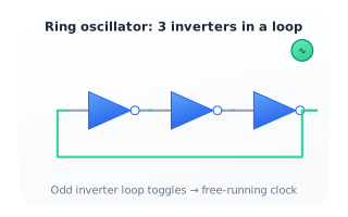
Connect an odd number of inverters in a loop and the circuit never settles: each stage forces the next to flip, so the ring oscillates and produces a free-running clock. The frequency depends on the number of stages and each gate's delay — a classic way to measure process speed.
Citations
- Shannon, C. E. (1938). A symbolic analysis of relay and switching circuits. Reference 1
- Mano, M. M., & Ciletti, M. D. (2018). Digital design: With an introduction to the Verilog HDL, VHDL, and SystemVerilog (6th ed.). Reference 2