PISO Shift Register
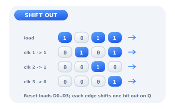
A PISO (parallel-in, serial-out) shift register does the opposite of a SIPO. Asserting Reset loads all N parallel D inputs into the register at once; then, on each rising clock edge, it shifts the word right and presents one bit at a time on the single serial Q output, least-significant bit first. After N clocks the whole word has been streamed out. PISO registers turn a parallel word into a serial stream, the transmitting half of parallel-to-serial conversion and the foundation of serial data links.
Load parallel, shift out serial
Set the D inputs with switches to form a word, then pulse Reset to load it. Now each rising clock edge pushes one bit out of the serial Q output, LSB first. Watch Q on an LED as you clock: it replays the loaded pattern one bit per edge. This is how a single wire can carry a whole byte over time.
| Clock | Q (out) | Register D3 D2 D1 D0 |
|---|---|---|
| reset (load 1011) | 1 | 1 0 1 1 |
| 1 | 1 | 0 1 0 1 |
| 2 | 1 | 0 0 1 0 |
| 3 | 0 | 0 0 0 1 |
| 4 | 1 | 0 0 0 0 |
Shifting right, LSB first
Internally each edge performs value = value >> 1, and Q always presents the current LSB. Because the least-significant bit leaves first, the receiving SIPO must reassemble the word in the same order. Match the two clocks and you have a complete link: PISO serialises on one end, SIPO deserialises on the other.
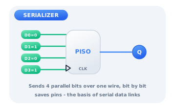
A parallel-to-serial link
Load a parallel word from several switches into the PISO, then clock it out over one wire to an LED or to a distant SIPO register. Sending N bits over a single line instead of N wires is exactly the trick behind SPI, UART and shift-register LED drivers: it trades time for pins, dramatically reducing the interconnect a system needs.
Citations
- Maity, H., Banerjee, S., Biswas, A., Pal, A., & Bhattacharjee, A. K. (2020). Design of reversible shift register using reduced number of logic gates. Micro and Nanosystems, 12(1), 42-48.. Reference 1
- Katz, R. H., & Borriello, G. (2005). Contemporary logic design (2nd ed.). Pearson Prentice Hall.. Reference 2